Products


Ceramic Substrates for Microelectronic Packaging
China-made Torbo® Ceramic Substrates for Microelectronic Packaging are widely utilized in electronic applications, such as converters, inverters, and power semiconductor modules, where they replace alternative insulating materials to reduce weight and volume and boost production output. They are also an essential element for extending the lifespan and dependability of the items they are utilized in because of their incredibly high strength.
Send Inquiry
Product Description
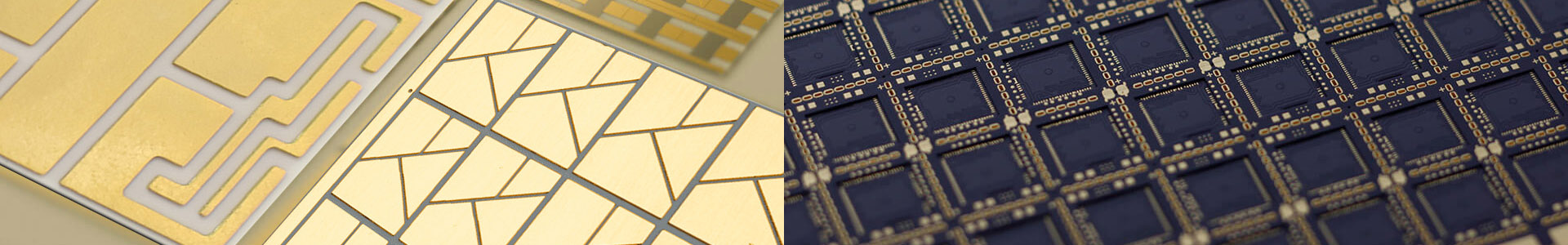
As the professional manufacturer, we would like to provide you Ceramic Substrates for Microelectronic Packaging.Ceramic Substrates for Microelectronic Packaging are flat, rigid, and often thin plates or boards made from ceramic materials, primarily used as a base or support for electronic components and circuits. These substrates are essential in various applications, including electronics, semiconductors, and other fields where heat resistance, electrical insulation, and mechanical stability are required. Ceramic substrates come in different shapes, sizes, and compositions to suit specific applications. They provide a stable and thermally conductive foundation for mounting and interconnecting electronic components, making them crucial for the performance and reliability of electronic devices and systems.
Color:Gray
Thickness:0.25-1mm
Surface processing:Double polished
Bulk density: 3.24g/㎤
Surface roughness Ra: 0.4μm
Bending strength: (3-point method):600-1000Mpa
Modulus of elasticity:310Gpa
Fracture toughness(IF method):6.5 MPa・√m
Thermal conductivity: 25°C 15-85 W/(m・K)
Dielectric loss factor:0.4
Volume resistivity: 25°C >1014 Ω・㎝
The Torbo® Ceramic Substrates for Microelectronic Packaging
Item:Silicon nitride substrate
Material:Si3N4Color:Gray
Thickness:0.25-1mm
Surface processing:Double polished
Bulk density: 3.24g/㎤
Surface roughness Ra: 0.4μm
Bending strength: (3-point method):600-1000Mpa
Modulus of elasticity:310Gpa
Fracture toughness(IF method):6.5 MPa・√m
Thermal conductivity: 25°C 15-85 W/(m・K)
Dielectric loss factor:0.4
Volume resistivity: 25°C >1014 Ω・㎝
Breakdown strength:DC >15㎸/㎜
Ceramic substrates for microelectronic packaging are specialized materials used in the manufacturing of microelectronic devices. Here are some features and applications of ceramic substrates:
Features:Thermal Stability: Ceramic substrates have excellent thermal stability and can withstand high temperatures without warping or degrading. This makes them ideal for use in high-temperature environments that are commonly found in microelectronics.Low Coefficient of Thermal Expansion: Ceramic substrates have a low coefficient of thermal expansion, making them resistant to thermal shock and reducing the possibility of cracking, chipping, and other damage that can occur due to thermal stress.Electrically Insulating: Ceramic substrates are insulators and have excellent dielectric properties, making them ideal for use in microelectronic devices where electrical isolation is required.Chemical Resistance: Ceramic substrates are chemically resistant and are not impacted by exposure to acids, bases, or other chemical substances, making them highly suitable for use in harsh environments.Applications:
Ceramic substrates are widely used in the manufacturing of microelectronic devices, including microprocessors, memory devices, and sensors. Some common applications include:LED Packaging: Ceramic substrates are used as a base for packaging LED chips due to their excellent thermal stability, chemical resistance, and insulating properties.Power Modules: Ceramic substrates are used for power modules in electronic devices such as smartphones, computers, and automobiles due to their ability to handle high power densities and high temperatures required for power electronics.High-Frequency Applications: Due to their low dielectric constant and low loss tangent, ceramic substrates are ideal for high-frequency applications such as microwave devices and antennas.Overall, ceramic substrates for microelectronic packaging play a significant role in the development of high-performance electronic devices. They offer exceptional thermal stability, chemical resistance, and insulating properties, making them highly suitable for a broad range of microelectronic applications.
Torbo®Ceramic Substrates for Microelectronic Packagingmanufactured in Chinese factories are widely used in electronic fields, such as power semiconductor modules, inverters and converters, replacing other insulating materials to increase production output and reduce size and weight. Their extremely high strength also makes them a key material for increasing the longevity and reliability of the products they use.
Double-sided heat dissipation in power cards (power semiconductors) , power control units for automobiles
Hot Tags: Ceramic Substrates for Microelectronic Packaging, Manufacturers, Suppliers, Buy, Factory, Customized
Product Tag
Send Inquiry
Please feel free to fill your inquiry in the form below. We will reply you in 24 hours.


We use cookies to offer you a better browsing experience, analyze site traffic and personalize content. By using this site, you agree to our use of cookies.
Privacy Policy